Step 1: Loading & Inspecting Gerber Files
Batch ZIP & Multi-File Drag-and-Drop
Drag and drop your complete PCB fabrication ZIP archive directly into the viewport. GerberPatch automatically unzips and categorizes Copper (.GTL/.GBL), Soldermask (.GTS/.GBS), Silkscreen (.GTO/.GBO), Drill (.DRL), and Board Outlines.
Layer Stackup, Visibility & Opacity
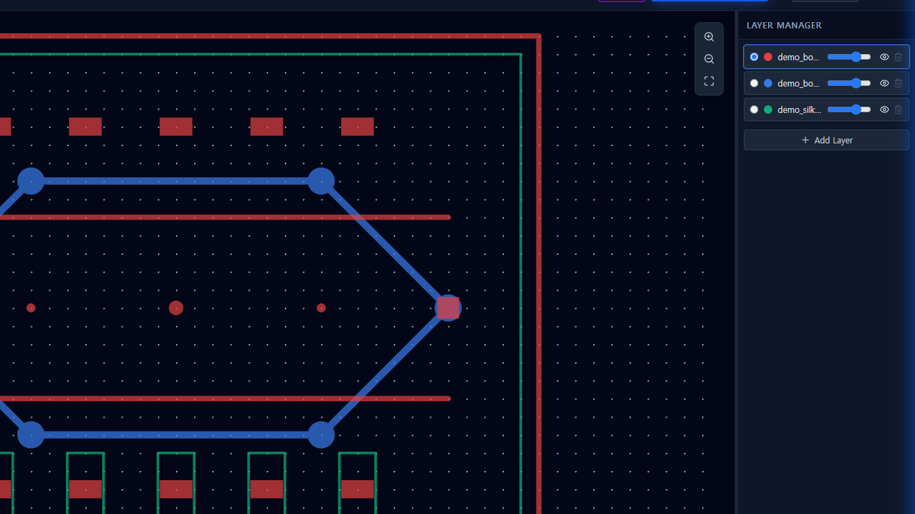
Toggle individual layer visibility with the eye icon in the right-side Layer Panel. Adjust individual layer opacity sliders to perform transparent X-ray inspections through multi-layer boards, click any layer's circular color chip to customize its palette with the native color picker, and drag layers vertically to reorder the physical visual stackup.
Visual Diff Mode
Activate Visual Diff mode to apply a difference blending pass between top and bottom copper layers or revision iterations, highlighting geometry discrepancies instantly.
Step 2: Viewer Environment & EDA Color Themes
Three Canvas Contrast Modes
Cycle through three calibrated viewport contrast modes using the floating HUD button or Settings modal:
- Deep Black (
#0a0a0c): High contrast for low-light environments and micro-trace inspection. - Dark Slate (
#1e293b): Ergonomic CAD standard backdrop to relieve eye fatigue during extended editing sessions. - Light Studio (
#f8fafc): High-luminance white backdrop optimized for documentation, PDF printing, and review snapshots.
Auto-Luminance Compensation: In Light Studio mode, high-luminance elements (white silkscreen #ffffff and pale yellow traces) automatically darken to high-contrast slate/charcoal (#0f172a) so markings never disappear into the white background.
Professional EDA Color Presets
Switch between industry-standard color conventions using the top-header Theme dropdown:
- Physical PCB (Green): Classic FR4 green solder mask (
65% opacity) overlaid on warm amber copper and crisp white silkscreen. - Classic CAD (Red / Blue): Standard dual-layer convention with primary red top copper and secondary blue bottom copper.
- High-Contrast (Teal / Coral): Vibrant modern palette engineered for high-density multi-bus routing.
- Multi-Layer Spectrum: Distinct 8-color spectrum per layer for complex multi-layer boards.
Physical PCB Stackup & Layer Color Customization
Layers are automatically ranked and stacked in natural physical order (Top Silk → Top Mask → Top Copper → Inners → Bottom Copper → Bottom Mask → Bottom Silk → Outline → Drill), allowing translucent soldermask to drape realistically over copper traces. Click any layer's circular color chip in the Layer Manager to launch the native color picker and define bespoke hex colors.
Mouse Wheel Zoom Direction Inversion
Customize your viewport interaction by toggling Invert Zoom (invertZoom) via the right floating toolbar or Settings modal. Your zoom preference is automatically saved to localStorage and preserved across sessions.
Step 3: Precision Inspection & Dimension LOD
Measure Tool (M) & Smart Snapping
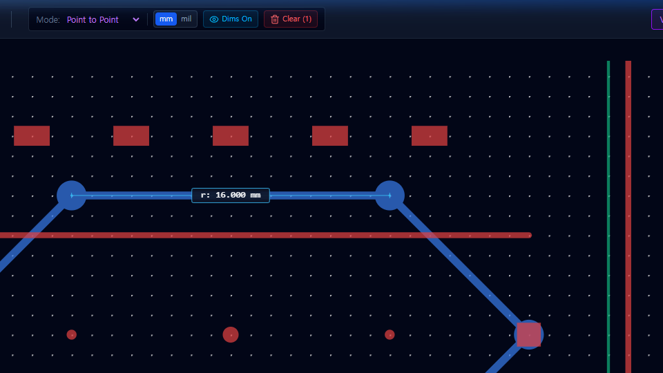
Press M or click the Ruler (Measure) tool and select any two points on the canvas to measure Euclidean distance, dx, dy, and angle in real time. Smart Magnetic Snap (S) automatically locks measurement probe pins onto pad centers and trace terminations.
Smart Level of Detail (LOD) Badges
When Zoomed-out, measurements automatically condense into a minimal distance badge (r: XX.XXX mm) to avoid cluttering dense board layouts. When Zoomed-in, badges expand into comprehensive 4-axis inspection data.
Persistent Annotations & Instant Unit Toggle (U)
Measurement annotations remain pinned to the canvas even when switching editing tools. Press U to toggle between mm and mil losslessly from anywhere. Measurement lines are strictly visual overlays and never alter exported fabrication files.
Step 4: Emergency Patching Tools
Trace / Line Routing with Magnetic Snap (S)
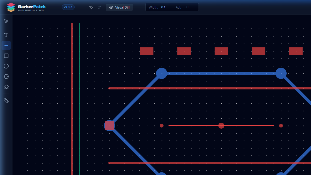
Use the Line / Trace tool to bridge hairline trace cracks or route engineering change order (ECO) jumpers. With Smart Magnetic Snap (S), trace start and end points latch seamlessly onto pad centers and existing trace endpoints without gap errors. Configure stroke thickness (0.1mm to 1.0mm+) in the sub-toolbar.
SMD Pads, Testpoints & Vias
Inject circular pads or rectangular SMD component targets on any copper layer. Set diameter or width × height to create standard 0402, 0603, or 0805 solderable jumper pads on the fly.
Text Markings & Layer Mirroring
Add revision markings (e.g., "REV 1.2", "ECO-FIX") in single-stroke vector fonts. Use the Mirror (Flip H) toggle to correctly orient text on bottom silkscreen or bottom copper layers.
Selective Copper Eraser with Real-Time Background Synchronization
Eliminate short-circuits or sever unwanted copper nets. The Eraser tool masks out targeted features natively in SVG and RS-274X, keeping surrounding ground planes and unconnected traces untouched. The eraser fill dynamically syncs with the active canvas background mode (Deep Black, Dark Slate, or Light Studio), preventing black rectangular artifacts and ensuring seamless visual cutouts across all themes.
Step 5: Multi-Select, Atomic Isolation & Transformations
Cross-Layer Click & Marquee Box Selection
In Select mode (Esc), click any trace or pad directly on the canvas without having to pre-select a layer on the right panel. Drag a marquee box to select multiple elements at once, or hold Shift / Ctrl to toggle items in and out of selection.
CAM350-Style Atomic Trace Isolation
Unlike standard Gerber viewers that group shared-aperture lines into monolithic paths, GerberPatch decomposes traces into atomic line segments. Selecting or deleting a trace segment affects only that specific segment—all other traces and pads sharing the aperture remain completely intact.
Drag-to-Move, Clipboard & Floating Mini Toolbar
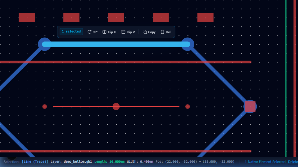
Grab any selected object and drag it across the board to reposition. Press Ctrl+C and Ctrl+V to duplicate elements with a clean +1.0mm board offset. Use the floating toolbar or keys (R rotate 90°, H flip horizontal, V flip vertical, Del delete). Press O to set a relative zero origin at the selection center.
Real-Time Vector Information Bar
The bottom-left status bar dynamically displays comprehensive vector metrics for both native Gerber elements and user patches: Type (Line, Circle, Rect), Layer filename, Euclidean Length (Length: XX.XXXmm), Width/Thickness, Diameter/Radius, and start/end coordinates.
Step 6: Smart Snapping, Crosshairs & Relative Origin
Smart Magnetic Snap Engine (S)
Toggle magnetic snapping with the S key or the toolbar Magnet button. The cursor magnetically latches to pad centers and copper trace endpoints with an interactive indicator ring, providing sub-millimeter precision for trace routing, pad placement, and distance checks.
Full-Screen Orthogonal Crosshairs (X)
Press X to activate full-screen orthogonal crosshair guides spanning the canvas. Perfect for visually checking trace collinearity, component pitch alignment, and symmetry across distant board coordinates.
User-Defined Relative Origin (O / Shift+O)
Press O to set a temporary relative zero datum (0, 0) at any snap point, cursor location, or selected object center. The status bar immediately reveals differential relative offsets (ΔX, ΔY) alongside absolute values. Press Shift+O or click Reset to return to the board origin.
Instant Unit Toggle (U) & Cheatsheet (?)
Toggle units on the fly between mm and mil using U with mathematical precision. Press ? anytime to open the built-in keyboard shortcut reference modal.
Step 7: Smart ZIP Export & Integrity Validation
Smart ZIP Re-packaging (Recommended)
When exporting an uploaded fabrication package, only modified layers are regenerated into fresh RS-274X Gerber commands. Untouched files—such as NC drill data (.drl), soldermask, silkscreen, and board outlines—remain 100% byte-for-byte identical to your original upload.
One-Click RS-274X Integrity Check
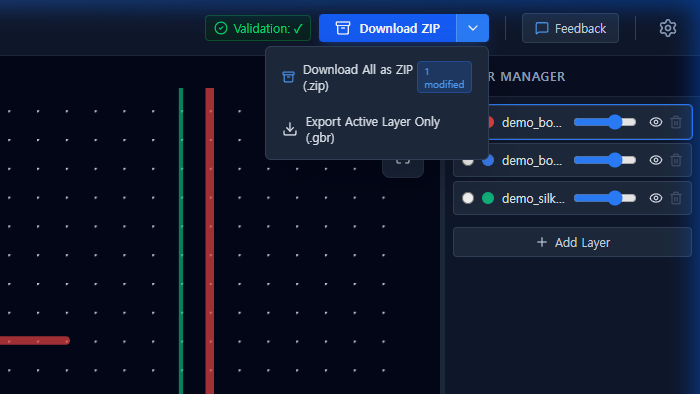
Click the Validate button in the header to run an internal RS-274X syntax and coordinate boundary audit. Once verified with a green checkmark (Validation: ✓), the download action is safely enabled.
Split Export Dropdown
Use the split button in the top-right header to choose between downloading the full bundled .zip archive or exporting only the active layer as a standalone .gbr file.
Step 8: Privacy-First Local Auto-Recovery & Session Management
100% Client-Side & Zero Server Transmission
Engineered strictly for confidential hardware development and NDA-governed intellectual property. All Gerber parsing, rendering, and caching occur exclusively within your browser's native IndexedDB storage. Your design files, layers, and coordinates are never uploaded to any remote server or cloud infrastructure.
Silent Background Auto-Save
Changes to your project—including loaded layers, customized palettes, visibility toggles, pan/zoom viewport coordinates, and newly drawn jumper traces—are silently debounced (1 second) and persisted in the background. No disruptive toast alerts or status bars interrupt your engineering workflow.
Instant 0ms Session Restoration
If you accidentally refresh your tab or close your browser, GerberPatch displays a non-intrusive recovery notification upon return:🔒 Local Browser Cache Found (No Server Upload) • N layers, M patches
Click Resume Session to instantly restore your workspace with pre-compiled SVG geometry (bypassing slow file re-parsing), while preserving the original binary Gerber Blobs for seamless RS-274X production export.
Workspace Reset via File Menu
Ready to work on a new PCB? Click the File ▾ menu in the top header and select New Project (Clear Session). An explicit confirmation dialog allows you to wipe all cached board data and patch items safely, returning you to a clean dropzone.
Previous session cached in browser. (4 layers, 3 patches)
Keyboard Shortcuts Cheat Sheet
Navigation & CAD Viewport
Edit, Transform & History
Tools, Coordinates & Precision
Smart Input Field Event Guarding
All single-letter shortcuts (X, S, O, U, M, R, H, V, ?) are automatically bypassed while typing inside text inputs, dimension text fields, or modal dialogs, preventing accidental tool switching during editing.